Sapphire
Other Materials
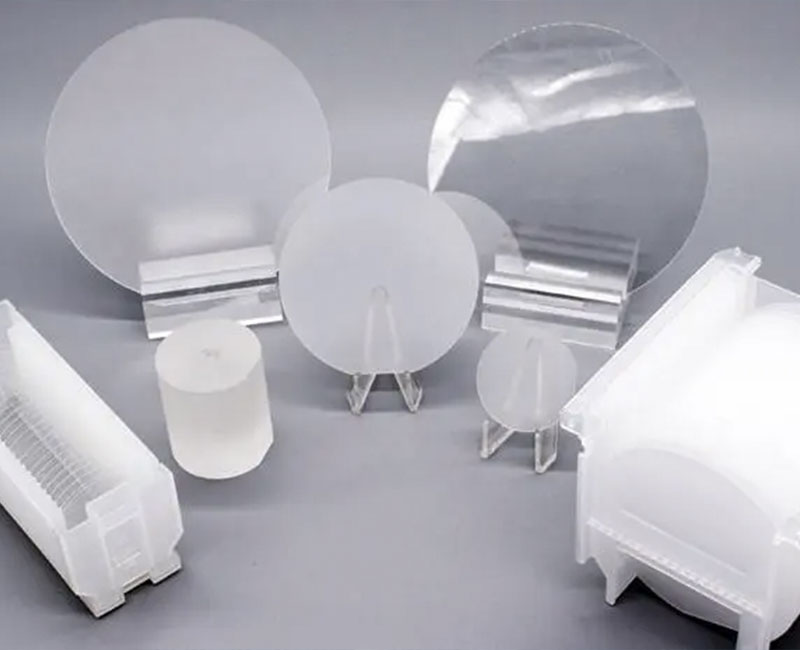
Size: 2 inches, 4 inches, 6 inches, and custom-cut pieces;
Orientations: C-axis, M-axis, R-axis; Single-side polished, double-side polished;
Thickness: 100um, 280um, 300um, 350um, 430u..
Description
- Size: 2 inches, 4 inches, 6 inches, and custom-cut pieces;
- Orientations: C-axis, M-axis, R-axis; Single-side polished, double-side polished;
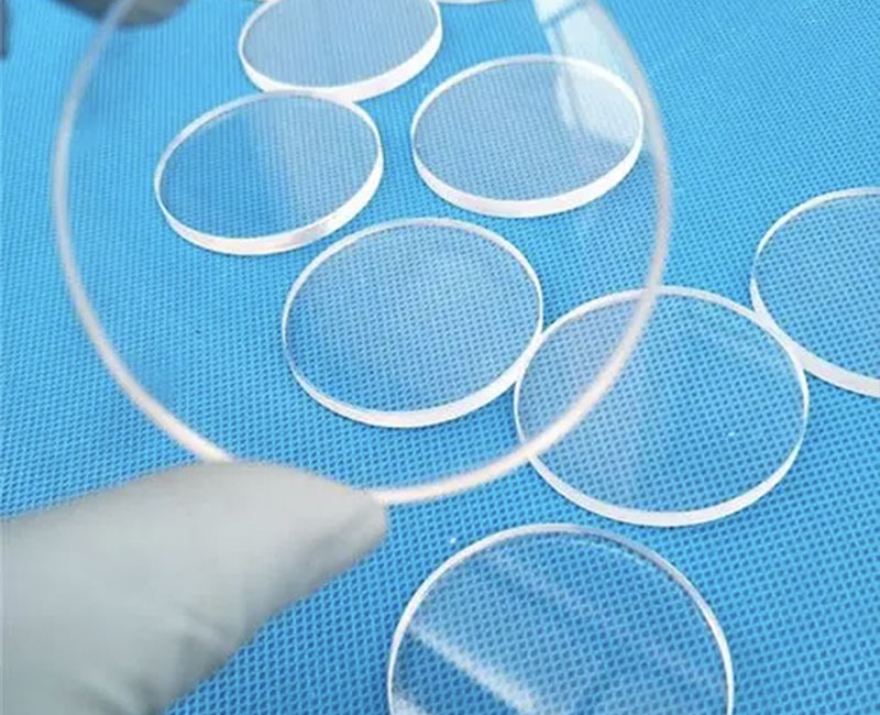
- Thickness: 100um, 280um, 300um, 350um, 430um, 500um, 650um, 1mm;
- Overview: Sapphire is a single crystal of aluminum oxide, the second-hardest material in nature after diamond. Sapphire exhibits excellent transparency, high strength, impact resistance, abrasion resistance, corrosion resistance, high-temperature resistance, and biocompatibility, making it suitable for various shapes. It is an ideal substrate material for manufacturing semiconductor optoelectronic devices.
- Applications: Sapphire single crystal is a versatile material widely used in industries such as industrial, defense, and research, including applications like high-temperature infrared windows. It is a preferred substrate in the LED and LD industries for blue, violet, and white light (requiring the epitaxial growth of gallium nitride films on sapphire substrates) and is also a crucial substrate for superconducting thin films, including high-temperature superconducting films such as Y-series and La-series. Additionally, it is utilized for growing practical MgB2 (magnesium diboride) superconducting films.
|
Crystal Orientation
|
C (0001)
|
R (1-102)
|
M (10-10)
|
A (11-20)
|
|||
|
Physical Properties
|
Crystallographic optical properties are present along the C-axis, while other axes have negative optical properties. The C-plane is a flat surface and is the preferred cutting plane.
|
Slightly more challenging to cut than A-plane.
|
The M-plane exhibits a stepped sawtooth structure, making it difficult to cut and prone to cleavage.
|
The hardness of the A-plane is significantly higher than that of the C-plane, showing resistance to wear and scratching, and it has a Z-shaped sawtooth surface that is relatively easy to cut.
|
|||
|
Applications
|
The C-axis sapphire substrate is used for the growth of III-V and II-VI family deposited films, such as gallium nitride, which can produce blue LED products, laser diodes, and applications in infrared detectors. This is mainly due to the mature and cost-effective process of growing sapphire crystals along the C-axis, with stable physical and chemical properties during epitaxial growth on the C-plane.
|
R-axis substrates, with differently deposited silicon materials, are used in microelectronic integrated circuits. Moreover, during the process of epitaxial silicon growth and film deposition, high-speed integrated circuits and pressure sensors can be formed. R-type substrates are also applied in the production of other superconducting components, high-resistance resistors, and gallium arsenide.
|
Primarily used for growing non-polar/semi-polar GaN epitaxial films to improve light-emitting efficiency.
|
The A-axis substrate produces a uniform capacitance/dielectric and is highly insulating, applied in hybrid microelectronics technology. High-temperature superconductors can be generated by A-type substrate crystal growth.
|
|||
|
Processing Capabilities
|
Patterned sapphire substrates (PSS): Designed and fabricated on sapphire substrates through growth or etching to create nano-level specific pattern structures for controlling the output light form of LEDs. This simultaneously reduces dislocation defects between GaN grown on sapphire substrates, improves epitaxial quality, and enhances the internal quantum efficiency and light extraction efficiency of LEDs. Additionally, various structural components such as sapphire prisms, lenses, apertures, cones, etc., can be custom processed as per customer requirements.
|
||||||
|
Properties
|
Density
|
Hardness
|
Melting Point
|
Refractive Index (Visible and Infrared Wavelengths)
|
Transmittance (Double-side Polished)
|
Dielectric Constant
|
|
|
3.98 g/cm³
|
9 (Mohs)
|
2053°C
|
1.762~1.770
|
≥85%
|
11.58 @ 300K at C axis (9.4 at A axis)
|
||


